INDIA'S FUTURE DIAMOND SEMICONDUCTOR COMPANY

About Atyabhuta

Atyabhuta Semiconductors is an MNIT Jaipur incubated deep-tech semiconductor startup focused on Diamond-on-Silicon wafers, single-crystal diamond semiconductor technology, advanced MPCVD systems, and futuristic semiconductor infrastructure.

Diamond is widely recognized as the 4th generation semiconductor material due to its exceptional thermal conductivity, ultra-wide bandgap, high breakdown voltage, and next-generation electronic performance.

MNIT JAIPUR INCUBATED STARTUP

Engineering India's Future Diamond Semiconductor Ecosystem

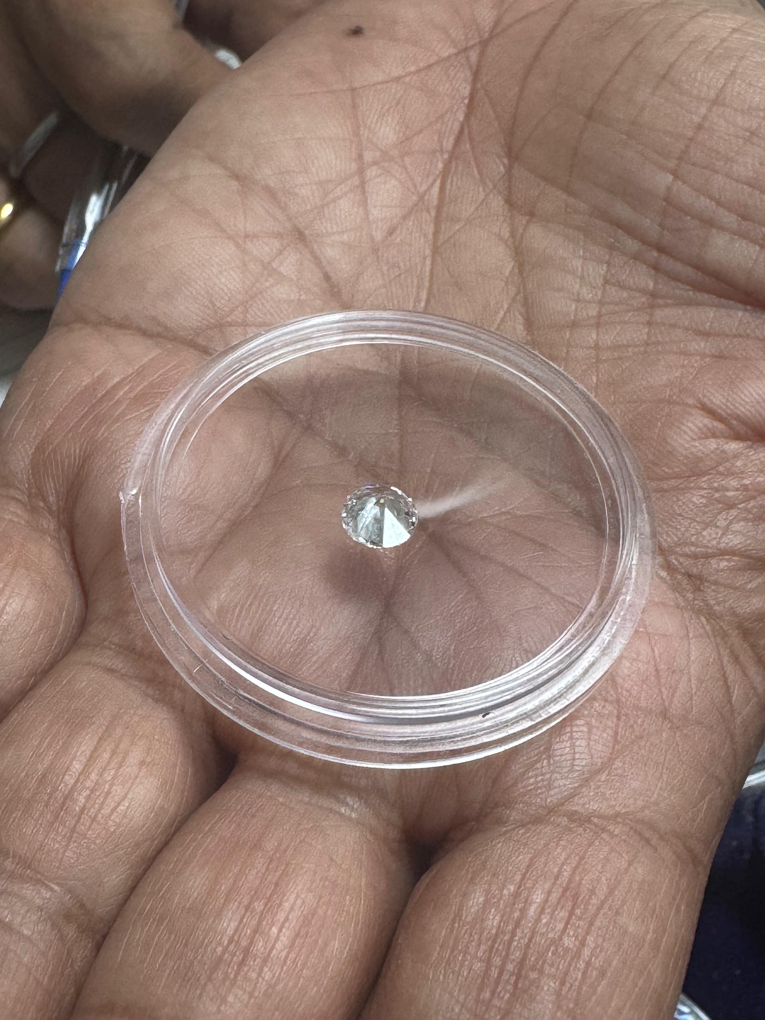
Atyabhuta Semiconductors is focused on the development and commercialization of advanced diamond semiconductor wafers for high-power electronics, RF systems, thermal management, and next-generation semiconductor applications.

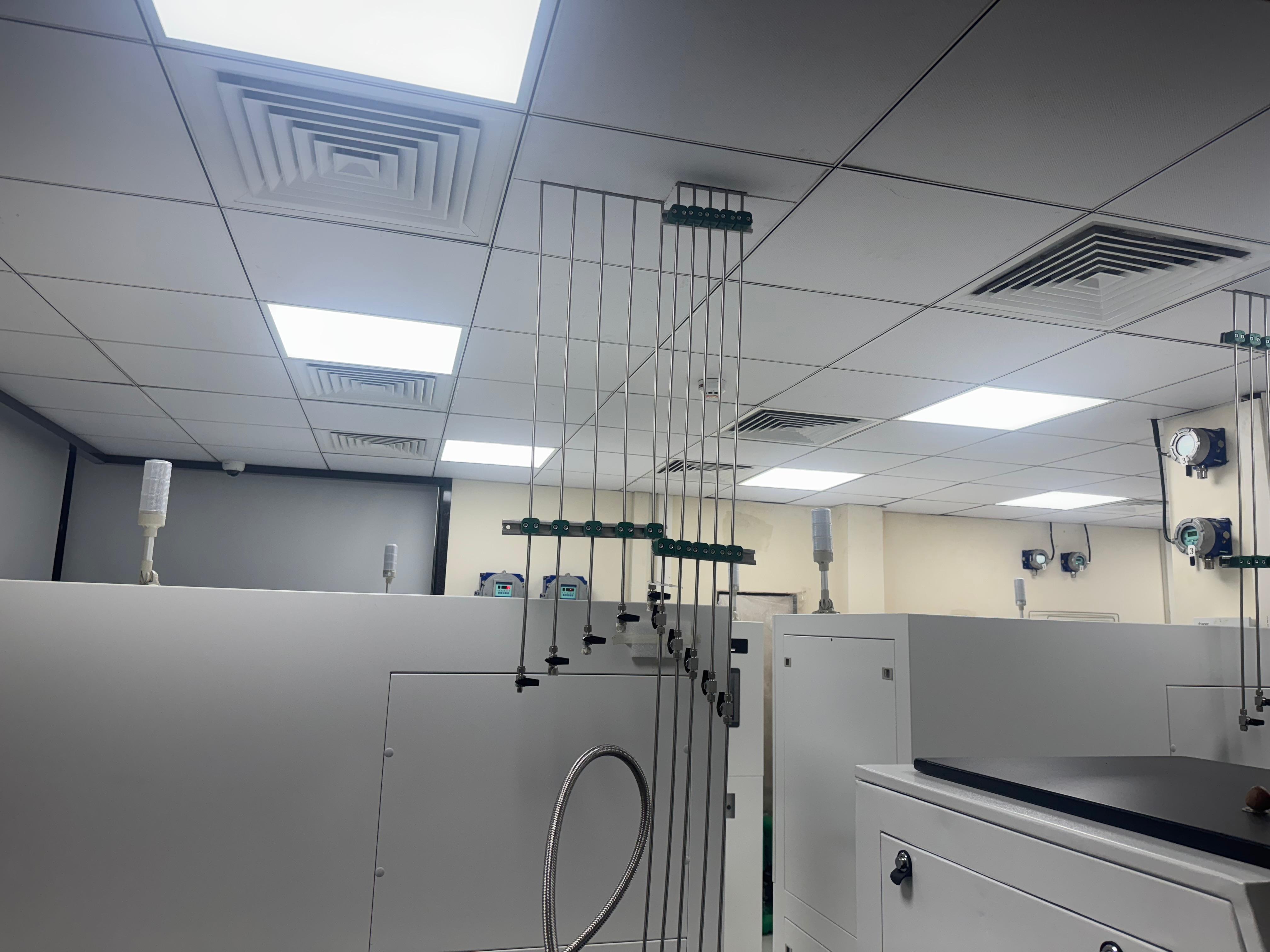
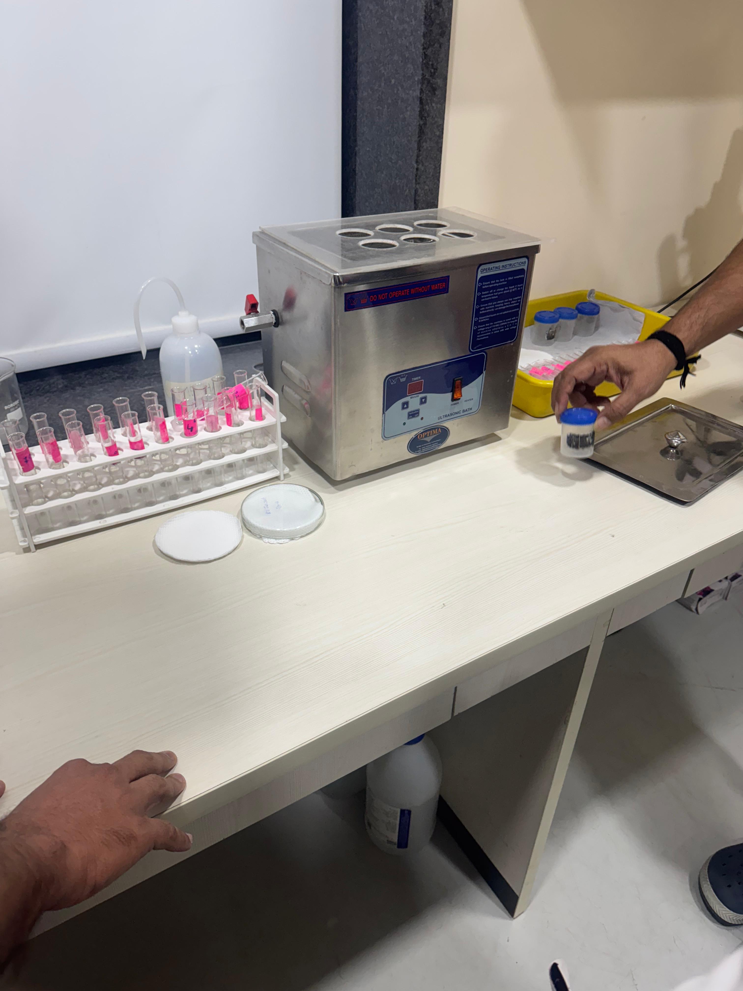
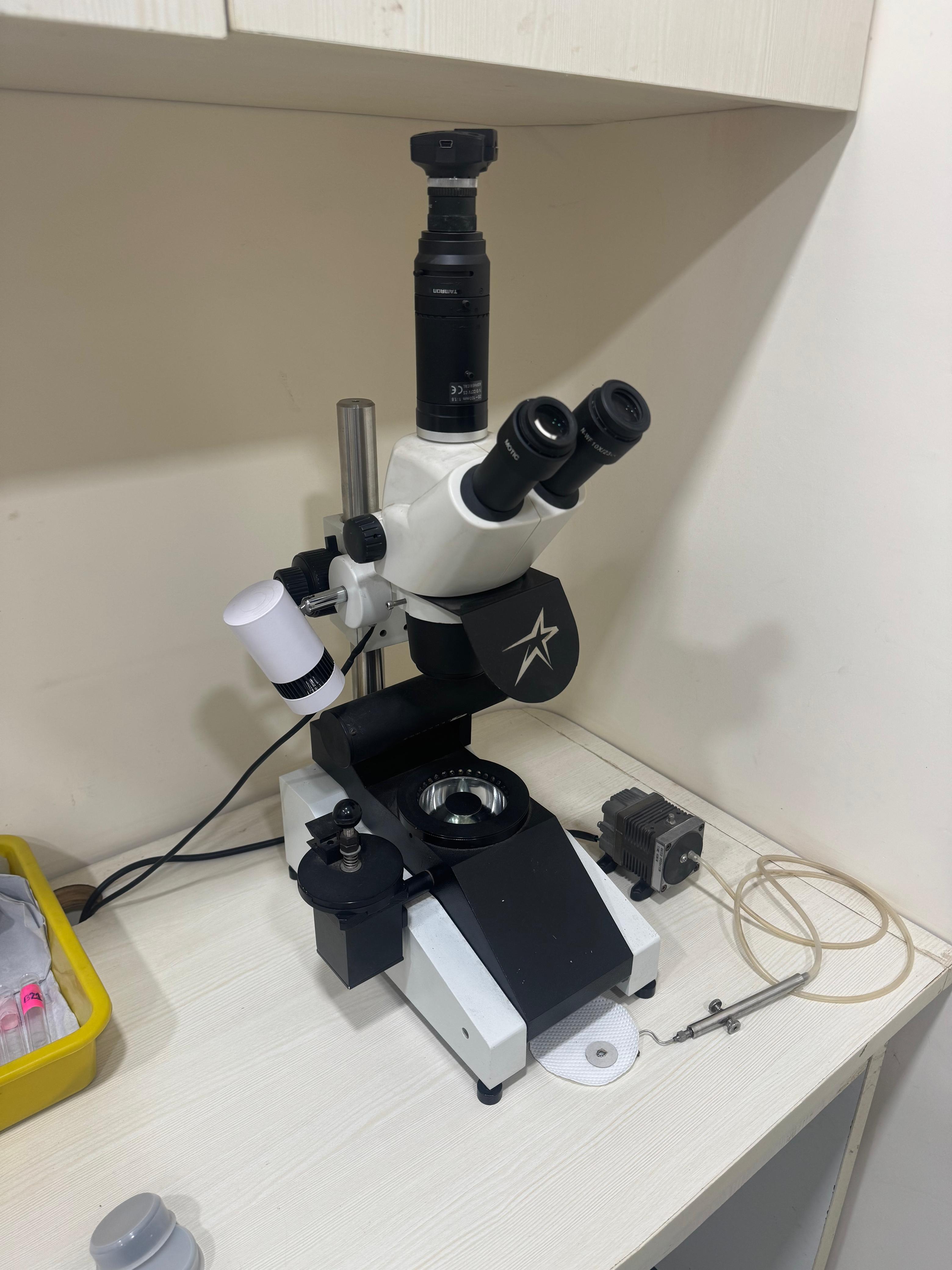
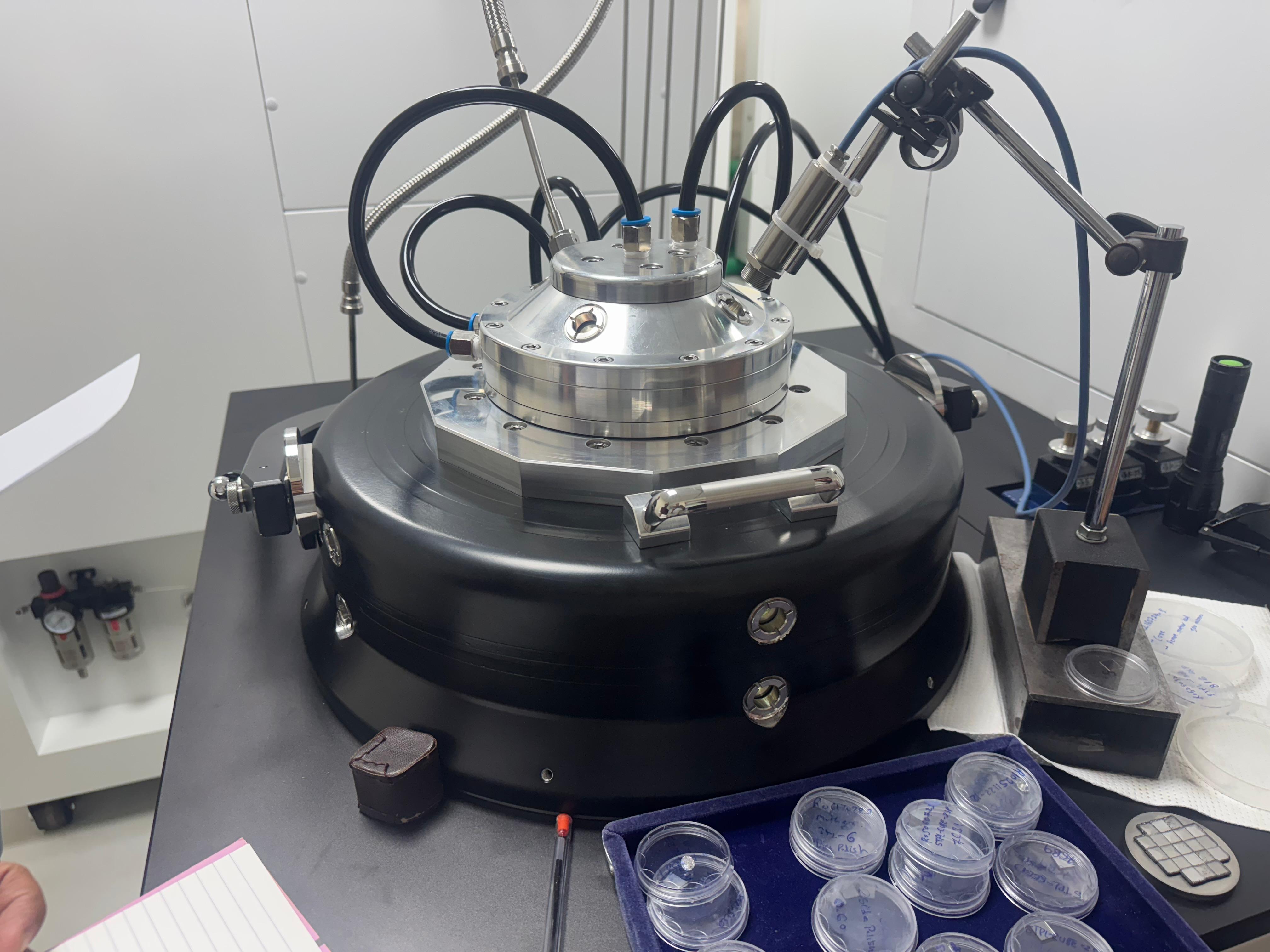
The company integrates semiconductor-grade MPCVD technology, precision plasma engineering, advanced wafer research, and deep-tech semiconductor innovation to build India's future diamond wafer ecosystem.

Technology Vision

Building India's future diamond semiconductor ecosystem.

MNIT

Incubated and supported through the MNIT Jaipur innovation and semiconductor research ecosystem.

4TH

Diamond is considered the fourth-generation semiconductor material for future electronics and high-power systems.

MPCVD

Advanced microwave plasma CVD systems designed for semiconductor-grade diamond wafer growth and engineering.

Research Infrastructure

Advanced semiconductor laboratories, wafer engineering environments, and futuristic diamond semiconductor systems.